Electronics, Photonics and ICT
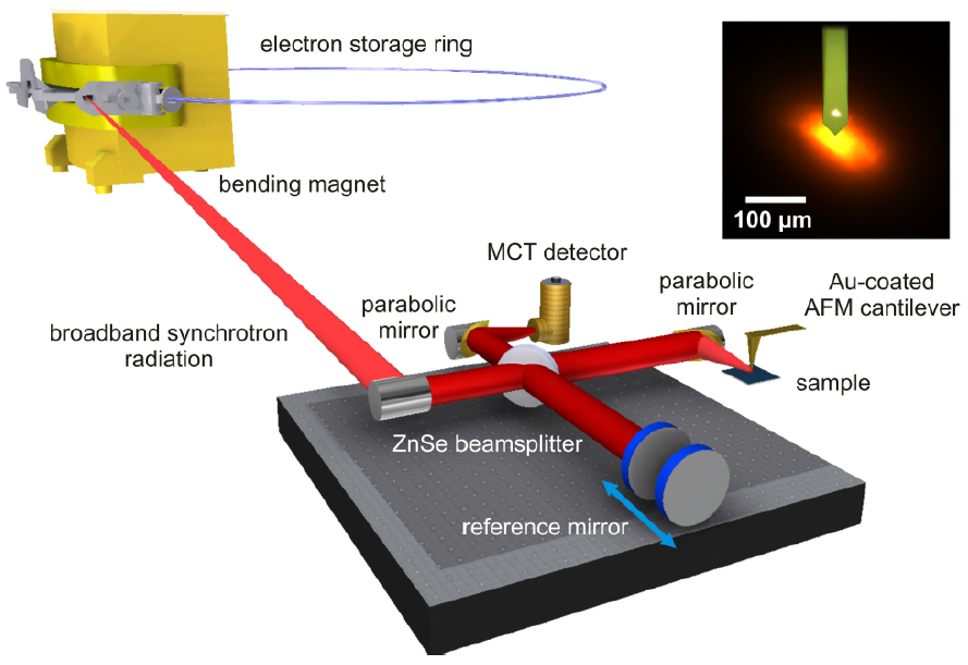
The electronics industry is constantly at the forefront of research and innovation aimed at improving the performance and energy efficiency of devices characterized by a constant trend towards miniaturization. Synchrotron light sources enable the study of nanoscale devices and characterize electronic materials with unprecedented spatial resolution. With X-ray nano probes and a beam size that can range between 20 and 100 nanometers, one can map electronic devices using a variety of techniques, including nano- and micro-tomography, nano-diffraction, nano-fluorescence and FTIR microscopy.
Synchrotron techniques provide answers to the following problems:
- Mechanical properties, including stress and strain on single crystals, polycrystalline materials, thin films, and epitaxial layers.
- Morphological and structural characterization, including multimodal analysis, film thickness, and roughness.
- Physico-chemical characteristics, including magnetic, band, and work functions.
- Failure analysis for bulk devices and thin films: voids, precipitates, dislocations and delamination.
- Microstructure: grain size distribution and a map of crystal orientation.
